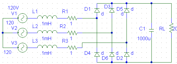
4.1 Circuit Representation.
The following diagram shows the practical three phase diode bridge rectfier.
Figure 6. Three phase diode bridge rectifier.
4.2 Description of Circuit Operation
A filter capacitor is connected to the dc side of the rectifier. The supply side transmission line is represented by the R and L in series. It is not very difficult to understand the operation of this circuit. The diodes are numbered according to the sequence in which they begin to conduct. Out of the diodes 1, 3 and 5 with common cathode connections, the diode connected to the highest positive phase voltage would conduct. Similarly, out of the diodes 2,4 and 6, with common anode connections, the diode connected to the most negative phase voltage would conduct. If the three phase voltage waveforms are drawn and examined, it will be easily seen that the diodes conduct in the sequence 1,2,3…and so on. Each diode conducts for 120 degrees per cycle, and a new diode begins to conduct after a 60 degree interval. The output waveform, Vd, which consists of portions of the line-to-line ac voltage waveforms, repeats with a 60 degree interval making it a six-pulse rectifier.
4.3 Circuit Representation for Pspice Simulation
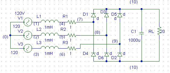
Figure 7. Three-phase diode bridge rectifier with nodes numbered for Pspice.
4.4 Pspice Code for three-phase diode bridge rectifier
The same diode model developed for the single phase rectifier has been used here as well. The rest of the codes are straight forward. To overcome convergence problem, some initial conditions have been assigned to the inductor current and capacitor voltage.
Practical Three-Phase, Diode-Bridge Rectifier
*3-phase voltages
V1 1 0 SIN(0 170V 60 0 0 0)
V2 2 0 SIN(0 170V 60 0 0 -120)
V3 3 0 SIN(0 170V 60 0 0 -240)
*ac-line inductance
LS1 4 1 0.1mH IC=2
LS2 5 2 0.1mH IC=2
LS3 6 3 0.1mH IC=2
*ac-line resistance
RS1 7 4 1000m
RS2 8 5 1000m
RS3 9 6 1000m
*load resistance and smoothing capacitor.
RLOAD 10 11 30.0
CD 10 11 1000uF IC=160V
*diode switches
D1 7 10 PDIODE
D3 8 10 PDIODE
D5 9 10 PDIODE
D4 11 7 PDIODE
D6 11 8 PDIODE
D2 11 9 PDIODE
*
.MODEL PDIODE D(IS=1E-10 N=1 BV=1200 IBV=10E-3 VJ=0.7)
.options abstol=1n reltol=0.01 vntol=0.01 itl5=120000
.TRAN 0.1m 1000m UIC
.PROBE
.END
4.5 Simulation Results
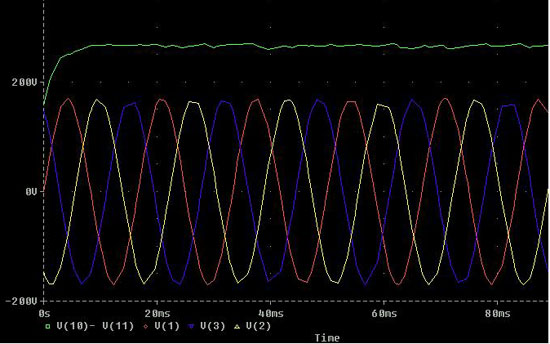
Figure 8. Output voltage compared with the 3-phase input voltage.
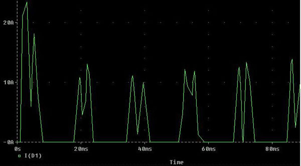
Figure 8. Current through diode D1.
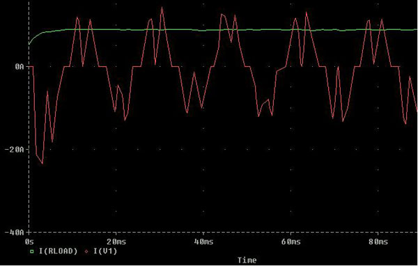
Figure 9. Current drawn from phase voltage V1 compared with the current drawn by the load resistor.
4.6 Interpretation
Figure 7 shows the output voltage compared with the input three phase voltages. By theory, we expect a six-pulse dc output. But here, the output is nearly a straight line. This is because of the effect of the filter capacitor that have been used. As expected, Figure 8 shows that a diode conducts for 120 degrees per cycle or per one period. Like the output voltage, the output current is also almost straight dc, while the shape of the current drawn from a phase voltage results from the different conduction cycles of the diodes.
